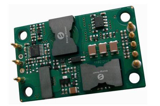
DC-DC Converters 100W Output 12V YN100-48S12-POC
Features
Output power: 100W
Wide input range: 36-72VDC
High conversion efficiency: Up to 93%
Line regulation to ±0.5%
Load regulation to ±0.5%
Fixed operating frequency
Isolation Voltage :1,500V
Enable (On/Off) Control
Output over-load protection
Hiccup mode short circuit protection
Over-temperature protection
Input under-voltage lock-out
Output voltage trim: ±10% Vout
Package: Open Frame
Quarter Brick: 2.2×1.37×0.42in
55.9×34.8×10.7mm
Product Overview
These DC-DC converter modules use advanced power
processing, control and packaging technologies to provide
the performance, flexibility, reliability and cost effectiveness
of a mature power component. High frequency Active Clamp
switching provides high power density with low noise and
high efficiency.
Product’s Introduction
The YN100 series is an independently regulated single output converter that uses the industry standard quarter brick package size. The very high efficiency is a result of ENARGY CORP patented topology that uses synchronous rectification and an innovative construction design to minimize heat dissipation and allow extremely high power densities. The power dissipated by the converter is so low that a heat sink is not required, which saves cost, weight, height, and application effort. All of the power and control components are mounted to the multi-layer PCB substrate with highyield surface mount technology, resulting in a more reliable product.
1. Electric Characteristics
Electrical characteristics apply over the full operating range of input voltage, output load (resistive) and base plate temperature, unless otherwise specified. All temperatures refer to the operating temperature at the center of the base plate.
1.1 Absolute maximum ratings
|
Parameter
|
Min
|
Typ
|
Max
|
Units
|
Notes
|
|
Input Voltage
|
|
|
|
78
|
Continuous, non-operating
|
|
|
|
|
75
|
Continuous, operating
|
|
|
|
|
78
|
Operating transient protection
|
|
Isolation voltage
|
|
|
|
2000
|
In to out;Basic insulation, Pollution
Degree 2
|
|
Operating Temperature
|
-55
|
|
|
100
|
M-Grade
|
|
Storage Temperature
|
-65
|
|
|
125
|
M-Grade
|
|
Enable to –Vin Voltage
|
-0.8
|
|
|
10
|
|
1.2 Input Characteristics
|
Parameter
|
Min
|
Typ
|
Max
|
Units
|
Notes
|
|
Operating input voltage
|
36
|
48
|
72
|
Vdc
|
Continuous
|
|
Input Surge Withstand
|
|
|
78
|
Vdc
|
<100mS
|
|
Under-Voltage Lockout
|
|
35.5
|
35.8
|
Vdc
|
Turn - On Threshold
|
|
32.5
|
34.0
|
|
Vdc
|
Turn - Off Threshold
|
|
Maximum Input Current
|
|
|
3.3
|
A
|
Full Load; Minimum Vdc Input
|
|
Efficiency
|
|
92
|
|
%
|
Figures 1-2
|
|
Dissipation, Standby
|
|
7
|
11
|
W
|
No Load
|
|
Disabled Input Current
|
|
|
10
|
mA
|
Enable pin low
|
|
Recommend External Input
Capacitance
|
|
100
|
|
uF
|
Typical ESR 0.1-0.2W, see Figure 4
|
1.3 Output Characteristics
|
Parameter
|
Min
|
Typ
|
Max
|
Units
|
Notes
|
|
Output Voltage Set point
|
11.88
|
12
|
12.12
|
V
|
Nominal input; No load;25℃
|
|
Output Current Range
|
0
|
|
8.33
|
A
|
Subject to thermal derating;
|
|
Line Regulation
|
|
±0.05
|
±0.50
|
%
|
Low line to high line; full load
|
|
Load Regulation
|
|
±0.09
|
±1.0
|
%
|
No load to full load; nominal input
|
|
Temperature Regulation
|
|
±0.002
|
±0.005
|
% / °C
|
Over operating temperature range
|
|
Current limit
|
8.8
|
9.5
|
11.2
|
A
|
Output voltage 95% of nominal
|
|
Short circuit current
|
0.3
|
9.5
|
10.8
|
A
|
Output voltage <250 mV
|
|
RMS
|
|
|
70
|
mVp-p
|
Nominal input; full load; 20 MHzbandwidth; p See Figures 3 & 4
|
|
Peak-to-Peak
|
|
|
100
|
mVp-p
|
|
Maximum Output Cap.
|
|
|
4000
|
μF
|
Nominal input; full load
|
1.4 Dynamic Response Characteristics
|
Parameter
|
Min
|
Typ
|
Max
|
Units
|
Notes
|
|
Change in Output Current
(di/dt= 0.1A/us)
|
|
|
400
|
mV
|
50% to 75% to 50% Iout max; Figure 7
|
|
Change in Output Current
(di/dt= 2.5A/us)
|
|
|
480
|
mV
|
50% to 75% to 50% Iout max; Figure 8
|
|
Settling Time
|
|
300
|
|
uS
|
To within 1% Vout nom.
|
|
Turn-on Time
|
|
15
|
|
mS
|
Full load; Vout=90% nom. Figure 5
|
|
Shut-down fall time
|
|
5
|
|
mS
|
Full load; Vout=10% nom. Figure 6
|
|
Output voltage overshoot
|
|
|
5
|
%
|
Nominal input; Full load;
|
1.5 Features Characteristics
|
Parameter
|
Min
|
Typ
|
Max
|
Units
|
Notes
|
|
Switching Frequency
|
200
|
230
|
260
|
KHz
|
Regulation stage and Isolation stage
|
|
Trim(Pin6)
|
See part 6.3 Voltage Trim(Pin6)
|
|
Output Voltage Trim
|
|
8
|
|
%
|
Trim Up, Trim Pin to (-) Vout.
|
|
|
8
|
|
%
|
Trim Down, Trim Pin to (+) Vout.
|
|
Enable(ON/OFF)Control(Pin2)
|
See part 6.1
|
|
Enable Voltage
Enable Source Current
|
|
|
10
|
Vdc
|
Enable pin floating
|
|
|
|
0.5
|
mA
|
|
|
Enable (On - Off Control)
Positive Logic
|
2.5
|
|
10
|
Vdc
|
On–Control, Logic high or floating
|
|
-0.5
|
|
2.0
|
Vdc
|
Off–Control, Logic low
|
1.6 Protections Characteristics
|
Parameter
|
Min
|
Typ
|
Max
|
Units
|
Notes
|
|
Over-Load Protection
|
105
|
115
|
130
|
%
|
Current–Mode, Pulse by Pulse Current
Limit Threshold,(%Rated Load)
|
|
Short – Circuit Protection
|
|
|
65
|
mΩ
|
Type: Hiccup Mode, Non–Latching,
Auto–Recovery,Threshold,Short–Circuit
Resistance
|
|
Over–Temperature
Protection
|
|
105
|
|
℃
|
Type: Non–Latching, Auto-Recovery;
Threshold, PCB Temperature
|
|
|
15
|
|
℃
|
Hysteresis
|
1.7 Safety Standard
|
Parameter
|
Min
|
Typ
|
Max
|
Units
|
Notes
|
|
Isolation Voltage
|
1,500
|
|
|
Vdc
|
In to Out
|
|
1500
|
|
|
Vdc
|
In to base
|
|
500
|
|
|
Vdc
|
Out to base
|
|
Isolation Resistance
|
10
|
|
|
MΩ
|
At 500VDC to test it when atmospheric
pressure and R.H. is 90%
|
|
Isolation Capacitance
|
|
1000
|
|
pF
|
|
2. Environmental Characteristics
|
Parameter
|
Min
|
Typ
|
Max
|
Units
|
Notes
|
|
Operating Temperature
|
-55
|
|
+100
|
℃
|
Extended, base PCB temperature
|
|
Storage Temperature
|
-65
|
|
+125
|
℃
|
Ambient
|
|
Temperature Coefficient
|
|
|
±0.02
|
%/℃
|
|
|
Humidity
|
20
|
|
95
|
%R.H.
|
Relative Humidity, Non - Condensing
|
|
Weight
|
|
1.4(40)
|
|
Oz (g)
|
Open Frame
|
|
MTBF ( calculated )
|
1
|
|
|
MHrs
|
TR-NWT-000332; 80% load,300LFM,
40℃ Ta
|
3. STANDARDS COMPLIANCE
|
Parameter
|
Notes
|
|
UL/cUl60950
|
File # E194341,Basic insulation & pollution degree 2
|
|
EN60950
|
Certified by TUV
|
|
72/23/EEC
|
|
|
93/68/EEC
|
|
|
Needle Flame Test (IEC 695-2-2)
|
test on entire assembly; board & plastic components UL94V-0 compliant
|
|
IEC 61000-4-2
|
ESD test, 8kV - NP, 15kV air - NP (Normal Performance)
|
|
GR-1089-CORE
|
Section 7 - electrical safety, Section 9 - bonding/grounding
|
|
Telcordia (Bell core) GR-513
|
|
·An external input fuse must always be used to meet these safety requirements. Contact Ours for official safety
certificates on new releases or download from the ENARGY CORP. website.
4. QUALIFICATION TESTING
|
Parameter
|
# Units
|
Test Conditions
|
|
Life Test
|
32
|
95% rated Vin and load, units at derating point, 1000 hours
|
|
Vibration
|
5
|
10-55Hz sweep, 0.060” total excursion,1 min./sweep, 120 sweeps for 3
axis
|
|
Mechanical Shock
|
5
|
100g minimum, 2 drops in x and y axis, 1 drop in z axis
|
|
Temperature Cycling
|
10
|
-40°C to 100°C, unit temp. ramp 15°C/min., 500 cycles
|
|
Power/Thermal Cycling
|
5
|
Tolerating = min to max, Vin = min to max, full load, 100 cycles
|
|
Design Marginality
|
5
|
Tmin-10°C to Tmax+10°C, 5°C steps, Vin = min to max, 0-105% load
|
|
Humidity
|
5
|
85°C, 85% RH, 1000 hours, 2 minutes on and 6 hours off
|
|
Solderability
|
15 pins
|
MIL-STD-883, method 2003
|
·Extensive characterization testing of all ENARGY CORP. Products and manufacturing processes is performed to
ensure that we supply robust, reliable product. Contact factory for official product family qualification document.
5. WORK CURVE&WAVE

Figure 1: Efficiency at nominal output voltage vs. load
current for minimum, nominal, and maximum input voltage
at 25°C.
Figure 2: Power dissipation at nominal output voltage vs.
load current for minimum, nominal, and maximum input
voltage at 25°C.
Figure 3: Output voltage ripple at nominal input voltage and
rated load current (20 mV/div). Load capacitance: 1μF
ceramic capacitor and 10μF tantalum capacitor. Bandwidth:
20 MHz. See Figure 13 & part 7th.
Figure 4: Test set-up diagram showing measurement points
for Input Terminal Ripple Current ( Test 1 ), Input Reflected
Ripple Current ( Test 2 ) and Output Voltage Ripple
(Figure 3).
Figure 5: Turn-on transient at full load (resistive load) (2
ms/div).Input voltage pre-applied. Ch 1: Vout (2V/div). Ch
2: ON/OFF input(5V/div)
Figure 6: Shut-down fall time at full load (2 ms/div).
Ch 1: Vout (2V/div)
Ch 2: ON/OFF input (5V/div)
Figure 7: Output voltage response to step-change in load
current (50%-75%-50% of Iout(max); dI/dt = 0.1A/μs). Load
cap: 10μF, 100 mW ESR tantalum capacitor and 1μF
ceramic capacitor. Ch 1: Vout (200mV/div), Ch 2: Iout
(10A/div).
Figure 8: Output voltage response to step-change in load
current (50%-75%-50% of Iout(max): dI/dt = 2.5A/μs). Load
cap: 470μF, 30 mW ESR tantalum capacitor and 1μF
ceramic cap. Ch 1: Vout (200mV/div), Ch 2: Iout (10A/div).
6. Pin Function Description
6.1 Enable (ON/OFF) Control (Pin 2):
The Enable pin allows the power module to be switched on and off electronically. The Enable (On/Off) function is
useful for conserving battery power, for pulsed power application or for power up sequencing.
The Enable pin is referenced to the -Vin. It is pulled up internally, so no external voltage source is required. An open
collector (or open drain) switch is recommended for the control of the Enable pin.
When using the Enable pin, make sure that the reference is really the -Vin pin, not ahead of EMI filtering or
remotely from the unit. Optically coupling the control signal and locating the opto coupler directly at the module will
avoid any of these problems. If the Enable pin is not used, it can be left floating (positive logic) or connected to the -Vin
pin (negative logic).Figure A details five possible circuits for driving the ON/OFF pin. Figure B is a detailed look of
the internal ON/OFF circuitry.
Figure A: Various circuits for driving the ON/OFF pin.
Figure B: Internal ON/OFF pin circuitry
6.2 Remote Sensing (Pins 7 and 5):
Remote sensing allows the converter to sense the
output voltage directly at the point of load and thus
automatically compensates the load conductor distribution &
contact losses (Figure C). There is one sense lead for each
output terminal, designated +Sense and -Sense. These leads
carry very low current compared with the load leads.
Internally a resistor is connected between sense terminal and
power output terminal. If the remote sense is not used, the
sense leads needs to be shorted to their respective output
leads(Figure D).
Figure C: Remote Sense Connection
Care has to be taken when making output
connections. If the output terminals should disconnect
before the sense lines, the full load current will flow down
the sense lines and damage the internal sensing resistors.
Be sure to always power down the converter before
making any output connections. The maximum
compensation voltage for line drop is up to 0.5V
Figure D: Remote Sense is not Used.
6.3 Voltage Trim (Pin 6):
Output voltage can be adjusted up or down with an external resistor. There are positive trim logic and negative
trim logic available. For positive logic, the output voltage will increase when an external trimming resistor is connected
between the Trim and +Vout/+Sense pin. The output voltage will decrease when an external trimming resistor is
connected between Trim and -Vout/-Sense pin. A multi-turn 20Ký trim pot can also be used to adjust the output voltage
up or down.(Figure E & F)
Table 6.3:Output Trim Logic
|
Output Trim Logic:
|
Positive Logic
|
Negative Logic
|
|
|
Optional - P
|
Standard
|
|
Trim-Up
|
Trim Pin to +Sense
|
Trim Pin to -Sense
|
|
Trim-Down
|
Trim Pin to -Sense
|
Trim Pin to +Sense
|
Figure E:Positive Trim Logic
Figure F: Trim Pot Connection
7. Basic Operation and Features Application
7.1 Output Ripple & Noise Test:
The output ripple is composed of fundamental frequency ripple and high frequency switching noise spikes. The
fundamental switching frequency ripple (or basic ripple) is in the 100KHz to 1MHz range; the high frequency switching
noise spike (or switching noise) is in the 10 MHz to 50MHz range. The switching noise is normally specified with 20
MHz bandwidth to include all significant harmonics for the noise spikes.
The easiest way to measure the output ripple and noise is to use an oscilloscope probe tip and ground ring pressed
directly against the power converter output pins, as shown below. This makes the shortest possible connection across
the output terminals. The oscilloscope probe ground clip should never be used in the ripple and noise measurement. The
ground clip will not only act as an antenna and pickup the radiated high frequency energy, but it will introduce the
common-mode noise to the measurement as well.
The standard test setup for ripple & noise measurements is shown in Figure F. A probe socket (Tektronix, P.N.
131.0258-00) is used for the measurements to eliminate noise pickup associated with long ground clip of scope probes.
Figure F: Ripple & Noise Standard Testing Means.
7.2 Typical application circuit
Figure G: Typical application circuit (negative logic unit, permanently enabled).
Application Circuits: Figure G below provides a typical circuit diagram which details the input filtering and voltage trimming.
7.3 Input Filtering
DC-DC converters, by nature, generate significant
levels of both conducted and radiated noise. There are two
types of conducted noise: common mode and differential
mode noise. The common mode noise is directly related to
the effective parasitic capacitance between the power
module input conductors and chassis ground. The
differential mode noise is across the input conductors. It is
recommended to have some level of EMI suppression to the
power module.
Conducted noise on the input power lines can occur as
either differential or common-mode noise currents. The
required standard for conducted emissions is EN55022
Class A (FCC Part15). (See Figure H)
Figure H: Input Filtering
7.4 Input Reflected Ripple Current
The converter is drawing current from input power source only when the input switch is on. This creates a pulsation current flow from the input source. The reflected ripple current is measured as a peak-to-peak current with a current probe over 0 to 20MHz bandwidth. Ripple current can be suppressed by an external Π (pi) filter as shown below. see Figure I.
Figure I: Input Reflected Ripple Current
7.5 Protection Features
·Input Under-Voltage Lockout: The converter is designed to turn off when the input voltage is too low, helping avoid an input system instability problem, The lockout circuitry is a comparator with DC hysteresis. When the input voltage is rising, it must exceed the typical Turn-On Voltage Threshold value(listed on the specification page) before the converter will turn on. Once the converter is on, the input voltage must fall below the typical Turn-Off Voltage Threshold value before the converter will turn off.
·Output Current Limit: The maximum current limit remains constant as the output voltage drops. However, once the impedance of the short across the output is small enough to make the output voltage drop below the specified Output DC Current-Limit Shutdown Voltage, the converter into hiccup mode indefinite short circuit protection state until the short circuit condition is removed. This prevents excessive heating of the converter or the load board.
·Over-Temperature Shutdown: A temperature sensor on the converter senses the average temperature of the module. The thermal shutdown circuit is designed to turn the converter off when the temperature at the sensed location reaches the Over-Temperature Shutdown value. It will allow the converter to turn on again when the temperature of the sensed location falls by the amount of the Over-Temperature Shutdown Restart Hysteresis value.
8. MECHANICAL DIAGRAM
NOTES:
1. Pins 4, 8 are 0.060” (1.52mm) dia. with 0.085” (2.16mm) dia. standoff shoulders.
2. All other pins are 0.040” (1.02mm) dia. with 0.065” (1.65mm) dia. standoff shoulders.
8.1 Pin Designations
|
Pin No.
|
Name
|
Function
|
|
1
|
Vin(+)
|
Positive input voltage
|
|
2
|
Enable
|
TTL input to turn converter on and off, referenced to Vin(-), with internal pull up.
|
|
3
|
Vin(-)
|
Negative input voltage
|
|
4
|
Vout(-)
|
Negative output voltage
|
|
5
|
Sense(-)
|
Negative remote sense. SENSE(-) may be connected to Vout(-) or left open.
|
|
6
|
Trim
|
Output voltage trim. Leave TRIM pin open for nominal output voltage.
|
|
7
|
Sense(+)
|
Positive remote sense. SENSE(+) may be connected to Vout(+) or left open.
|
|
8
|
Vout(+)
|
Positive output voltage
|

 Your message must be between 20-3,000 characters!